Introduction to I2C Communication
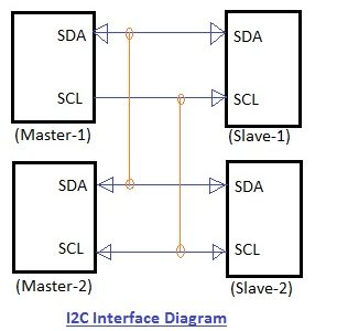
I2C combines the best features of SPI and UARTs. With I2C, you can connect multiple slaves to a single master (like SPI) and you can have multiple masters controlling single, or multiple slaves. This is really useful when you want to have more than one microcontroller logging data to a single memory card or displaying text to a single LCD.
This bus standard is developed by Philips initially to provide more hardware circuit efficiency and simplicity.
The I2C protocol supports multiple masters but usually there will be one master and more than one slaves. The master controls the clock signal and device which is addressed by it, is known as slave. There is 7 bit address used for slave device.
Each I2C-compatible hardware slave device comes with a predefined device address, the lower bits of which maybe configurable at the board level. The master transmits the device address of the intended slave at the beginning of every transaction. Each slave is responsible for monitoring the bus and responding only to its own address. This addressing scheme limits the number of identical slave devices that can exist on an I2C bus without contention; with the limit set by the number of user-configurable address bits (typically two bits, allowing up to four identical devices).
I2C is half duplex communication so you cannot send and receive data at same time. that why it has only one data line SDA.
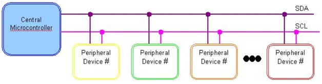
The I2C bus physically consists of 2 active wires and a ground connection. The active wires, called SDA and SCL, are both bidirectional. SDA is the Serial DAta line, and SCL is the Serial CLock line. Every device hooked up to the bus has its own unique address, no matter whether it is an MCU, LCD driver, memory, or ASIC. Each of these chips can act as a receiver and/or transmitter, depending on the functionality. Obviously, an LCD driver is only a receiver, while a memory or I/O chip can be both transmitter and receiver.
The I2C bus is a multi-master bus. This means that more than one IC capable of initiating a data transfer can be connected to it.
The I2C protocol specification states that the IC that initiates a data transfer on the bus is considered the Bus Master, which generally is a microcontrollers. Consequently, at that time, all the other ICs are regarded to be Bus Slaves.
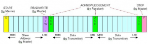
First, the MCU will issue a START condition. This acts as an ‘Attention’ signal to all of the connected devices. All ICs on the bus will listen to the bus for incoming data.
Then the MCU sends the ADDRESS of the device it wants to access, along with an indication whether the access is a Read or Write operation (Write in our example). Having received the address, all IC’s will compare it with their own address.
If it doesn’t match, they simply wait until the bus is released by the stop condition (see below). If the address matches, however, the chip will produce a response called the ACKNOWLEDGEMENT signal.
Once the MCU receives the acknowledgement, it can start transmitting or receiving DATA. In our case, the MCU will transmit data. When all is done, the MCU will issue the STOP condition.
This is a signal that the bus has been released and that the connected ICs may expect another transmission to start any moment.
I2C Configuration
i. The Start and Stop Configuration
A few note about start and stop conditions:
I) A single message can contain multiple Start conditions. The use of this so-called “repeated start” is common in I2C.
II)A Stop condition ALWAYS denotes the END of a transmission. Even if it is issued in the middle of a transaction or in the middle of a byte. It is “good behavior” for a chip that, in this case, it disregards the information sent and resumes the “listening state”, waiting for a new start condition
ii) Transmitting a byte to a slave
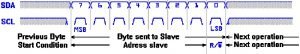
Once the START condition has been sent, a byte can be transmitted by the MASTER to the SLAVE.
This first byte after a start condition will identify the slave on the bus (address) and will select the mode of operation. The meaning of all following bytes depends on the slave.
iii) Receiving a byte from a slave
Once the slave has been addressed and the slave has acknowledged this, a byte can be received from the slave if the R/W bit in the address was set to READ (set to ‘1’).
The protocol syntax is the same as in transmitting a byte to a slave, except that now the master is not allowed to touch the SDA line.
Prior to sending the 8 clock pulses needed to clock in a byte on the SCL line, the master releases the SDA line. The slave will now take control of this line. The line will then go high if it wants to transmit a ‘1’ or, if the slave wants to send a ‘0’, remain low.
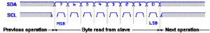
The meaning of all bytes being read depends on the slave. There is no such thing as a “universal status register”. You need to consult the data sheet of the slave being addressed to know the meaning of each bit in any byte transmitted.
iv) Getting Acknowledgement from a Slave
When an address or data byte has been transmitted onto the bus, then this must be ACKNOWLEDGED by the slave(s). In case of an address: If the address matches its own, then only that slave will respond to the address with an ACK. In case of a byte transmitted to an already addressed slave, then that slave will respond with an ACK as well.
The slave that is going to give an ACK pulls the SDA line low immediately after reception of the 8th bit transmitted, or, in case of an address byte, immediately after evaluation of its address. In practical applications this will not be noticeable
SDA
This means that as soon as the master pulls SCL low to complete the transmission of the bit,
SDA will be pulled low by the slave.
SCL
The master now issues a clock pulse on the SCL line (3). the slave will release the SDA line
upon completion of this clock pulse..
Serial Peripheral Interface (SPI)
SPI Overview
SPI is a general-purpose synchronous serial interface. During an SPI transfer, transmit and receive data is simultaneously shifted out and in serially. A serial clock line synchronizes the shifting and sampling of the information on two serial data lines.
Motorola created the SPI port in the mid 1980’s to use in their microcontroller product families. The SPI is mainly used to allow a microcontrollers to communicate with peripheral devices such as E2PROMs.
Devices communicate using a master/slave relationship, in which the master initiates the data frame. When the master generates a clock and selects a slave device, data may be transferred in either or both directions simultaneously.
In fact, as far as SPI is concerned, data are always transferred in both directions. It is up to the master and slave devices to know whether a received byte is meaningful or not.
So a device must discard the received byte in a “transmit only” frame or generate a dummy byte for a “receive only” frame.
SPI specifies four signals: clock (SCK1); master data output, slave data input (SI1); master data input, slave data output (SO1); and chip select (CS). Figure 1 shows these signals in a single-slave configuration. SCK1 is generated by the master and input to all slaves.
SI1 carries data from master to slave. SO1 carries data from slave back to master. A slave device is selected when the master asserts its CS signal.
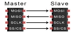
If multiple slave devices exist, the master generates a separate slave select signal for each slave.
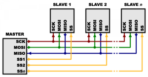
The majority of SPI devices provide these four lines. Sometimes it happens that SDI and SDO are multiplexed, for example in the temperature sensor LM74 from National Semiconductor, or that one of these lines is missing. A peripheral device which must or can not be configured, requires no input line, only a data output. As soon as it gets selected it starts sending data. In some ADCs therefore the SDI line is missing (e.g. MCCP3001 from Microchip).
There are also devices that have no data output. For example LCD controllers (e.g. COP472-3 from National Semiconductor), which can be configured, but cannot send data or status messages.
SPI Configuration
Because there is no official specification, what exactly SPI is and what not, it is necessary to consult the data sheets of the
components one wants to use. Important are the permitted clock frequencies and the type of valid transitions.
There are no general rules for transitions where data should be latched. Although not specified by Motorola, in practice four modes are used. These four modes are the combinations of CPOL and CPHA. In table 1, the four modes are listed.
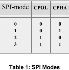
If the phase of the clock is zero, i.e. CPHA = 0, data is latched at the rising edge of the clock with CPOL = 0, and at the falling edge of the clock with CPOL = 1. If CPHA = 1, the polarities are reversed. CPOL = 0 means falling edge, CPOL = 1 rising edge.
The micro controllers from Motorola allow the polarity and the phase of the clock to be adjusted. A positive polarity results in latching data at the rising edge of the clock. However data is put on the data line already at the falling edge in order to stabilize. Most peripherals which can only be slaves, work with this configuration. If it should become necessary to use the other polarity, transitions are reversed.
4. Summary
| SPI | I2C |
| 1) Three bus lines are required; a data input line (SI1), a data output line (SO1) and a serial clock line (SCK1) [plus 1 Chip Select (CS)]
2) No official specification (component dependent) 3) Higher data rates (up to 10 MHz or more) 4) More efficient in point-to-point (single master, single slave) applications 5) Lack of built-in device addressing 6) Does not have an acknowledgement mechanism to confirm receipt of data. 7) Less overhead when handling point-to-point application 8) Suited better for applications that are naturally thought of as data streams | 1) Two bus lines are required; a serial data line (SDA) and a serial clock line (SCL) 2) With official specification (I2C protocol created by Philips) 3) Support transfer speeds of around 100kHz (original standard, or 400kHz using the most recent standard) 4) More efficient in multi-master, multi-slave applications 5) Built-in addressing scheme and straightforward 6) Have an acknowledgement mechanism to confirm receipt of data 7) More overhead when handling point-to-point application 8) Suited better for communication with on-board devices that are accessed on an occasional basis. |
I will address remaining minutiae in our future posts.
Until then, stay tuned and muchas gracias.
![]()