The invention of the Printed Circuit Board (PCB) was a big leap for the electronics and technology industries as it allowed electronic devices to be reduced to a more comfortable and practical size. PCB’s also decreased the human error. With smartphones and other portable devices flourishing, it is not surprising that the boards have become smaller to match mobile and miniaturized devices. Fortunately, the size of the PCB’s is inversely related to its features and capabilities. Now, most PCB’s are equipped with high-performance processors, HD video cards, etc.
PCB is used to mechanically support and electrically connect electronic components using conductive pathways, tracks or signal traces etched from copper sheets laminated onto a non-conductive substrate.
- It is also referred to as Printed Wiring Board (PWB) or etched wiring board.
Two purposes
A place to mount the component
Provides the means of electrical connection between the components
PCB’s can be
- Single sided (one copper layer)
- Double sided (two copper layers)
- Multi-layer
PCB is considered better than the design on bread board and more reliable.
So the bread board could be a way to test the hardware but could not be considered as final implementation
PCB Terminology
- Pad: a small surface of copper where component will be soldered to the board
- Via: plated hole that allows the current to pass thru the board
- Track (trace): conductive path connecting 2 points (pads, vias)
- Soldermask: a layer of insulating lacquer covering both surfaces of the board to prevent the solder to short circuit two tracks from different nets.
- Silkscreen (overlay): letters printed on the final board, e.g., solder mask
PCB Process Flow
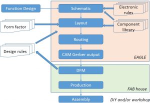
PCB Design steps
Stuff I Need To Get Started
- A Plan
- Block Diagram / Napkin Sketch
- Component Selection
- Connections and Testing Considerations
- Power and Performance Considerations
- A New Project
- Access to Libraries
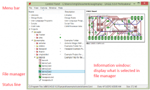
Eagle PCB

A CAD Tool For Designing a Board
Eagle is a very professional tool for designing PCB’s and allow the designer to import some of the design rule check of a manufacturer that will implement the in reality. Eagle is also giving options to the designer to create schematic for the circuit and design for best layout PCB board by routing wires either on one side or both sides to generate double sided PCB’s.
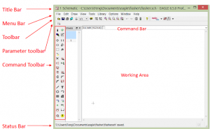
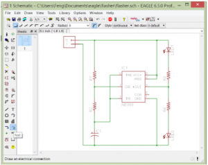
EAGLE Schematic
Eagle Schematic is away to represent the circuit diagram in a certain way to be represented simply after that on a PCB.
![]()
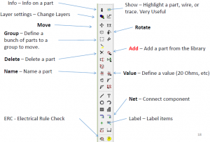
EAGLE SCHEMATIC FUNCTIONS
![]()
EAGLE Layout
Eagle Layout is a way to represent the eagle schematic in a finalized layout of a PCB which will be printed on it.
![]()
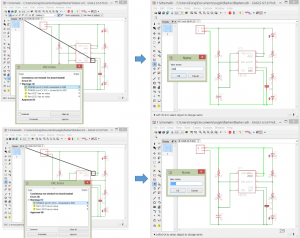
Creating a New Project
- Launch Eagle
- File -> New -> Project
- Enter Project Name
- Directory structure taken care of automatically.
- Active project is shown with a green light.
- Save it right away.
- Don’t worry about creating a Board just yet.
- Keep the 100-mil grid.
- Click the Add icon
- Find the component in the library
- Set values
- Don’t see the library? Try Use -> Library
- Click the Add icon
- Find the global symbol in the library (supply1)
- Place as if it were a component
- Click the Wire icon
- Have at it!
![]()
Some General Tips
- Avoid changing the grid unless absolutely necessary.
- Free Eagle version does not allow “sheets”.
- Free Eagle version requires that schematic drives the layout … not vice-versa.
- Groups, Info, and Layers icons are useful.
- Pan, zoom, niceties easy to use.
- Really care about that “net”? Label it.
- Document!
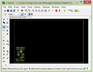
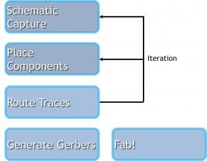
Place Components
Creating a new board design
- From the schematic, choose File -> Switch to Board.
- “Create From Schematic”? You bet!
- Board window automatically opens.

![]()
![]()
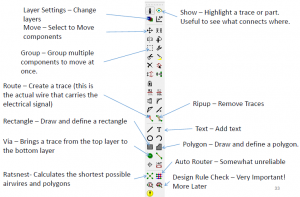
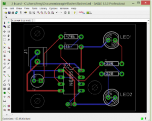
Route Traces
- You want to route, not wire.
- You want to ripup, not delete nets.
- Are you on the top or the bottom?
- Vias are on top and bottom. Easy to add.
- DRC often!
- Iterate like mad.
![]()
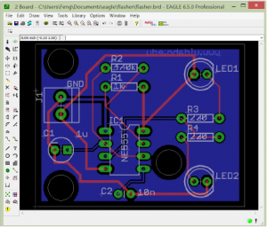
Some General Tips
- Two layers? Have an x-layer and a y-layer.
- Don’t forget mounting holes, other nice things.
- Add testability features.
- Do the “what if?” dance.
- Do the cardboard mockup.
- Pour Copper.
![]()
Autorouter
•[Board] Autorouter
![]()
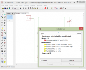
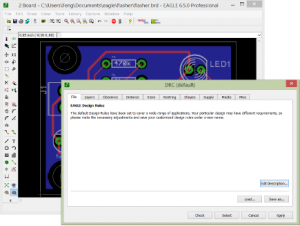
Design Rule Checker
[Board]DRC
![]()
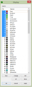
CAD Layers
1 Top (top tracks)
•16 Bottom (bottom tracks)
•17 Pads
•18 Vias
•19 Unrouted
•20 Dimension
•21 tPlace(top silkscreen)
•22 bPlace(bottom silkscreen)
•23 tOrigins
•24 bOrigins
•25 tNames
•26 bNames
•27 tValues
•28 bValues
•44 Drills (for pads (of through hole components) and vias)
•45 Holes (for mounting holes)
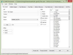
Gerber File Generation –CAM Processor [Board] File->CAM Processor
[CAM Processor] File->Open->Job->sfe-gerb274x.cam
The Gerber format is an open 2D binary vector image file format. It is the standard file used by Printed Circuit Board (PCB) industry software to describe the printed circuit board images: copper layers, solder mask, legend, etc.
•A 2D vector image format
•Universal format and industry standard for PCB fabrication
•TXT files with coordinates that tell the PCB machines to go to location X, Y and do something (drill, expose, etch, print, etc).
•Formats:
•RS-274X (Extended Gerber or X-Gerber)
•Human readable ASCII format consisting of a sequence of commands and coordinates
•RS-274D (obsolete)
•Different text files for different layers.
•Generated by the CAM (computer aided manufacturing) processor
PROCESS:
•[Board] File->CAM Processor
•[CAM Processor] File->Open->Job->sfe-gerb274x.cam
•[CAM Processor] Process Job
pro
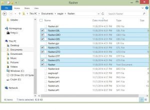
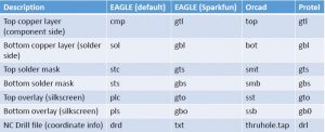
Typical Gerber File Types
![]()
Extension Layer
pcbname.GTL Top Copper
pcbname.GTS Top Soldermask
pcbname.GTO Top Silkscreen
pcbname.GBL Bottom copper
pcbname.GBS Bottom Soldermask:
pcbname.GBO Bottom Silkscreen:
pcbname.TXT Drills
pcbname.GML/GKO *Board Outline:
4 layer board also need
pcbname.GL2 Inner Layer2
pcbname.GL3 Inner Layer3
Notes: Gerber file must be RS-274X format. Drill file(pcbname.TXT) should be Excellon format.
FAB
Before you hit “the button” …
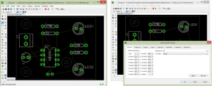
- Generate a Parts List (aka “The BOM”) using Export -> Partlist.
- Generate a Pin List (aka “The Netlist”) using Export -> Netlist.
- Sanity check both.
The PCB Design Process
A Summary of a Lot of Information
I will address remaining minutiae in our future posts.
Until then, stay tuned and muchas gracias.
![]()